


Molecular Dynamic Simulations of Nanowires
In materials science it is important to improve processing procedures and to predict the properties of materials based on those processing procedures. There are occassions when experimental investigation of processing and properties is difficult or costly. In such cases computational models are a fitting substitute. In addition investigation with computational models has a history of scientists discovering nuances in their models that previsously went unnoticed. Also, when the turn around time per simulation is lower and cheaper than the physical experiment, scientists can perform more experiements and ask more questions in the same amount of time. I believe that modern science can only benefit from computation.
Below I made molecular dynamic simulations of nanowires under compression. I simulated their response under compression and then was able to make predications about the young's modulus of the nanowires based on their radius. In conclusion, I found that the young's modulus of the nanowires was greater than that of bulk wires, as the radius decreased towards the nanoscale. In the simulations below the nanowires had a radius of 15 nanometers (nm). Where 1nm = 10^-9m.
This is a simulation of a gold nanowire (NW) under compression at 0.1nm per picosecond. It buckled nicely as a response.
In this simulation I compressed the NW faster at 0.5nm per picosecond. The atoms had less time to buckle nicely like before. The impulse was so great that the NW was crushed upon itself.
In this simulation I made the atoms hydrogen instead of gold. As you might expect the hydrogen atoms expanded to maintain equal pressure, at room temperature.
Photolithography
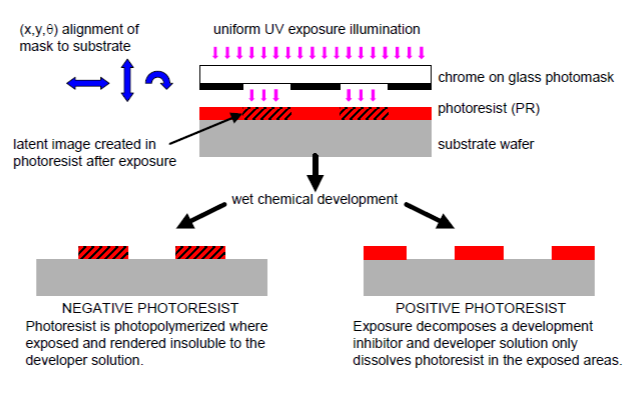
Photolithography is a very important processing method. Photolithography and its variants are used to create integrated circuits that power our electronic deveices, and are used to make small mechanical parts in nanotechnology research. There are three basic steps in photolithography outlined in the image below. First, make a reflective mask, with some protions of the mask that are transparent. Second, create a positive or negative photresist and apply it to a silicon substrate. Third place the mask above the substrate and expose the sandwich to ultra-violet light. It is imperative at this step to use the laws of optics to focus the UV light onto a space on the substrate smaller than the transparent portions of the mask. That demagnification, has been able to create integrated circuits as small as 12nm, that's really tiny! But with tinier junctions means more transistors can fit onto a single integrated circuit making it capable of more computations. Going back to the processing: Depending on the type of photoresist used the next step will differ slightly. However, either way, after UV exposure part of the photoresist dissolves away. Then an acid can be used to etch the pattern deeper into the substrate.
Some helpful optics are the resolution (R) and depth of field (DOF).
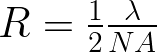
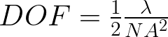
The challenge is to find a balance between the two for your application. With a lens of smaller f-number (equivalent to a larger numerical aperature (NA)) the resolution value and the depth of field values decrease. But a small R means two points that distance can be resolved In other words a small R means you can see the object better. In contrast a high depth of field is desirable. The DOF is the distance between planes normal to the object being viewed, that the object can be resolved.
Here is a photo of when I performed photlithography on a silicon wafer in UC Merced's clean room: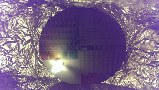
References:
[1] http://www.lifesci.boun.edu.tr/en/merkez_altyapilari/item/5_fotolitografi
Capacitor Electrodes of Polymer Coated + Metal Loaded, Carbon Nanofiber
Capacitors are important circuit elements with high power density, meaning they can release energy very fast yet are limited in their energy storage capability. Batteries have the opposite characteristics as capacitors. Nanotechnology is being used to create novel electrodes that will increase the energy density of capacitors, resulting in super-capacitors. A super-capacitor would have high power density and high energy density. In the lab I prepared carbon nanofiber electrodes, then coated the electrodes with a polymer grafting and baked the polymer so that the chains curled up or burned off leaving behind pits that metal nanoparticles would cling to. Then using cyclic voltammetry variants - oxidation reducation reaction(ORR) and oxidation evolution reaction (OER), I compared the changes in capacitance before and after metal loading.
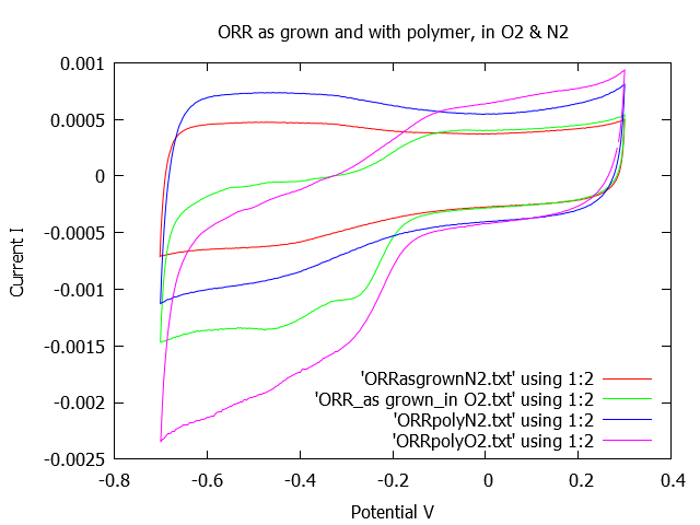
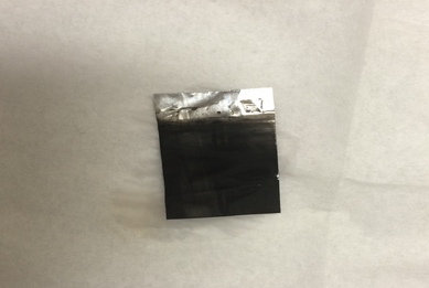
To the left are the ORR curves generated from two different electrodes, before and after using a polymer graft to load metal particles onto the electrodes. To the right is one of the electrodes I made at UC Merced. The work or the energy stored in a capacitor is proportional to the capacitance. The capacitance is proportional to the surface area of the electrode. In traditional materials the surface area is limited by the geometry of the electrode; however, using carbon nanofibers the surface becomes wavy. The wavy surface is full of the fibers growing on the metal surface. The wavy-fibers tend to have greater surface area than the electrode without carbon nanofiber. In addition the polymer + metal particles increase the area and increase the conductivity of the electrode. All in an effort to reach high power density and high energy density.
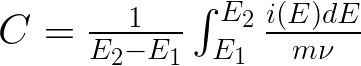
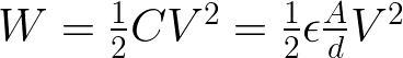
The goal of this research is to increase the capacitance and thus the total energy that can be stored in a capacitor. The following equations indicate that the capacitance can be calculated by integrating the ORR and OER curves, and relates the total energy stored (W), to the capacitance (C) and how capacitance is related to the electrode surface area (A).
References:
[1] Enhanced capacitance of manganese oxide via confinement inside carbon nanotubes Wei Chen, Zhongli Fan, Lin Gu, Xinhe Bao, and Chunlei Wang. Royal Society of Chemistry, 2010.
[2] chemwiki.ucdavis.edu/Analytical_Chemistry/Electrochemistry/Redox_Chemistry/Oxidation-Reduction_Reactions
 This website Rocketurtlestars.co is licensed under a Creative Commons Attribution-ShareAlike 4.0 International License.